FSB Motherboard Architecture
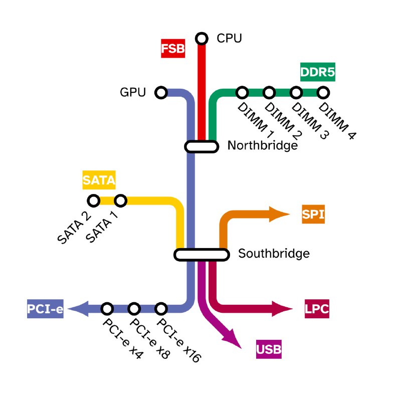
FSB CPU GPU DDR5 DIMM 1 DIMM 2 DIMM 3 DIMM 4 Northbridge SATA SATA 2 SATA 1 SPI Southbridge PCI-e PCI-e x4 PCI-e x8 PCI-e x16 LPC USB
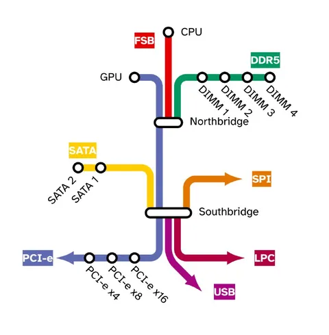
A humorous motherboard architecture diagram labels the front-side bus “FSB,” alongside the CPU, GPU, northbridge, southbridge, memory, storage, and expansion interfaces. The joke comes from the accidental association of FSB with Russia’s Federal Security Service, making a technical hardware diagram look faintly governmental or surveillance-related.
motherboard diagram / схема материнской платыCPU / процессорGPU / видеокартаnorthbridge / северный мостsouthbridge / южный мостDDR5 memory / память DDR5DIMM slots / слоты DIMMSATA ports / порты SATAPCI Express slots / слоты PCI ExpressUSB connector / разъём USBLPC bus / шина LPCSPI bus / шина SPIcolored circuit lines / цветные линии цепейarrow / стрелка
- @gentoomemes / 15187 2024-12-15
- Type
- image
- Size
- 786×800 · 52.5 KiB
- Mood
- absurd, technical
- Language
- en
- Added